John Wiley & Sons Inc
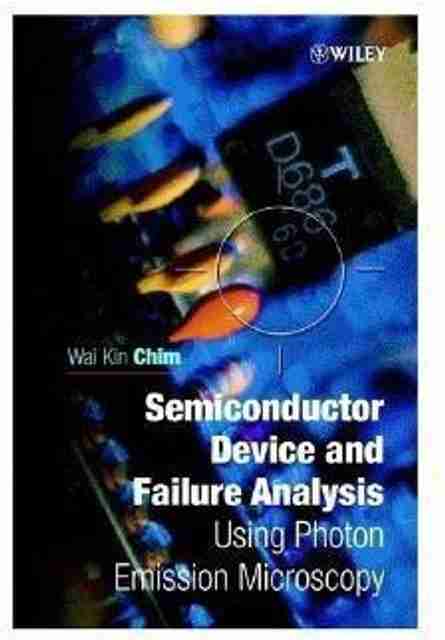
Semiconductor Device and Failure Analysis (English, Hardcover, Ch...
more
Buy at ₹23,320
Apply offers for maximum savings
Apply offers for maximum savings!
Apply for Card and Instant EMI
Product highlights
Title
Semiconductor Device and Failure Analysis
Imprint
John Wiley & Sons Inc
Product Form
Hardcover
Publisher
John Wiley & Sons Inc
Source ISBN
9780471492405
Genre
Technology & Engineering
ISBN13
9780471492405
Book Category
Higher Education and Professional Books
All details
Features, description and more
Specifications
Description
Manufacturer info
Show More
Questions and Answers
No questions and answers available
Be the first to ask about this product
Ask a question
Buy with EMI
From ₹864/m
B
u
y
a
t
₹
0
1
2
3
4
5
6
7
8
9
0
1
2
3
4
5
6
7
8
9
,
0
1
2
3
4
5
6
7
8
9
0
1
2
3
4
5
6
7
8
9
0
1
2
3
4
5
6
7
8
9
Hang on, loading content


